Centre for Functional Materials(CFM)

All Events
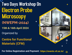
Two days Workshop on Electron Probe Microscopy (NWEPM-2024)

Two days Workshop on Electron Probe Microscopy(NWEPM-2024)
Click Here to View More

Two days National Workshop on X-Ray Diffraction & Rietveld Refinement (NWXRD-2023)

Two days National Workshop on X-Ray Diffraction & Rietveld Refinement (NWXRD-2023)
Click Here to View More

International Conference on Functional Materials for Future Technologies 2023(ICFMFT-2023)
Click Here to View More

Five Days Hands On Training on Density Functional Theory and its Applications using Gaussian 16

Click Here to View More


National Workshop

Five Days Hands On Training on Density Functional Theory and its Applications using Gaussian 16

Click Here to View More


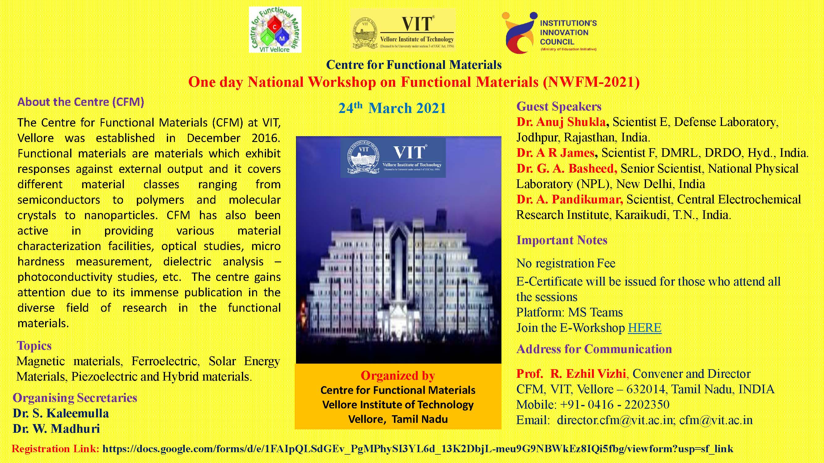
One day National Workshop on Functional Materials (NWFM-2021)
CFM-Workshop

Schedule

Inauguration
Welcome note and Introductory remarks
By
Dr. R. Ezhil Vizhi
Director, CFM

9:30AM - 9:55AM

Chairperson: Dr. R. Ezhil Vizhi

  Speaker Title Timing
1 Dr. Anuj Shukla Scientist E, Defense Laboratory, Jodhpur, Rajasthan, India. Functional Materials for Defence Application 10:00 AM -11:30 AM

Chairperson: Dr. S. Kaleemulla

2 Dr. A R James Scientist F, DMRL, DRDO, Hyderabad, India. Research in DMRL on Nano-materials: Piezoelectrics & Ferroelectrics 11:30 AM - 01:00 PM

Chairperson: Dr. Madhuri W

3 Dr. G. A. Basheed Senior Scientist, National Physical Laboratory (NPL), New Delhi,India Racetrack Memory Devices: Trapping and Injecting Single Domain Walls inMagnetic Wire 02:00 PM - 03:30 PM

Chairperson: Dr. S. Madeswaran

4 Dr. A. Pandikumar Scientist, Central Electrochemical Research Institute, Karaikudi, T.N.,India. Heterojunction Functional Materials for Photoelectrocatalytic WaterSplitting" 3:30 PM - 05:00 PM

Vote of Thanks
By
Dr. Madhuri W

05:00 PM - 05:05 PM


Note: After every talk the participants can interact with the speakers and discuss.


Session 1 (10:00 AM -11:30 AM)

Title: Functional Materials for Defence Application

Dr. Anuj Shukla
Scientist E, Defense Laboratory, Jodhpur, Rajasthan, India.

Read Abstract

DRDO's impetus for exploring functional materials is primarily for enhanced lethality or increased survivability of military objects. Functional materials are materials that have one or more properties that can be utilized in a controlled fashion by external stimuli and therefore applied in a broad range of applications. Functional materials are found in all classes of materials: ceramics, metals polymers, organic molecules, nanomaterials and metamaterials. In this lecture, two different classes of functional materials: (i) nanomaterials such as iron oxide nanoparticles, core-shell nano alloy, carbon nanoballs, graphene and their defense application; (ii) metamaterials as absorbers, metamaterials in form of quick response (QR) code, which can carry information such as texts/image, metamaterials for health monitoring of polymer composites will be presented and discussed.

About the Speaker

Dr. Anuj Shukla
Dr. Anuj shukla received his master of science in physics from the lucknow university and he accomplished his ph.d. In soft matter physics from martin-luther university, germany. He has joined drdo in 2009 as a scientist ‘d’ under talent search nri scheme.
Dr. Shukla has more than 20 years of research experience in synthesis and characterization of nano-structured materials at world’s leading institute in europe. His major research efforts in nanoscale materials include microemulsions, synthesis of magnetic nanoparticles, including core-shell structures, graphenic materials, radar absorbing materials and metamaterials as microwave absorbers, etc.
Dr. Shukla has published more than 50 articles in international journals and has presented more than 30 papers at international conference in Europe and India.


Session 2 (11:30 AM - 01:00 PM)

Title: Research in DMRL on Nano-materials: Piezoelectrics & Ferroelectrics

Dr. A R James
Scientist F, DMRL, DRDO,Hyderabad, India

Read Abstract

The fascinating area of Piezoelectrics and Ferroelectrics will be highlighted in this refresher course lecture. The Physics of such materials from the structural and electrical point of view will be described and then details of how such materials can be synthesized in the bulk ceramic and thin film forms, with emphasis on a very recent technique called Pulsed Laser Deposition (PLD) will be explained. Efforts in our lab to fabricate prototypes of various materials both in the bulk and thin film forms will be presented

About the Speaker

Dr. A. R. James
Dr. A. R. James is presently working as a Scientist ‘F’ in the Ceramics & Composites Group of Defence Metallurgical Research Lab (DMRL, DRDO), Hyderabad.
He has done his M. Sc and Ph. D. in Physics from Osmania University (1997).
He then worked as a Post Doctoral Fellow at the Max Planck Institute of Microstructure Physics in Germany (15.3.99-25.11.99), on the growth and characterization of large area epitaxial, ferroelectric thin films for Non-Volatile Ferroelectric Random Access Memories (NVFRAMs).
Thereafter, he was a Post Doctoral Fellow at the Materials Research Lab, at the Pennsylvania State University, USA from 1999-2001, wherein he worked on the development of ultra high strain piezoelectrics, for the Office of Naval Research, Washington DC, and Frequency Agile Materials for Microwave Electronics under DARPAs FAME program.
Upon his return to India, he worked as a Scientist at the Solid State Physics Lab, (DRDO) Delhi (from 2001-2004).
His current interests are in the field of soft piezoelectric ceramics, thin films and microwave ferroelectrics.
He has more than 90 publications in International journals and conference proceedings, and 5 patents to his credit.
He has 20 years Research Experience on Ferroelectric, magnetic and magnetoelectric materials.
He has authored three book chapters, all of International publishers.
He is a Governing Council member of the Materials Research Society of India.
He has delivered several lectures both in India and abroad and is a recipient of the prestigious MRSI award and will be delivering an invited lecture at the Indian Science Congress as well.


Session 3 (02:00 PM - 03:30 PM)

Title: Racetrack Memory Devices: Trapping and Injecting Single Domain Walls in Magnetic Wire

Dr. G. A. Basheed
Senior Scientist, National Physical Laboratory (NPL), New Dehli, India

Read Abstract

A single domain wall (DW) moves at linearly increasing velocity under an increasing homogeneous drive magnetic field. Present experiments show that the DW is braked and finally trapped at a given position when an additional antiparallel local magnetic field is applied. That position and its velocity are further controlled by suitable tuning of the local field. In turn, the parallel local field of small amplitude does not significantly affect the effective wall speed at long distance, although it generates tail-to-tail and head-to-head pairs of walls moving along opposite directions when that field is strong enough.

About the Speaker

Dr. G. A. Basheed
Dr. G. Abdul Baheed awarded Ph.D. from Central University Hyderabad under the guidance of Prof. S. N. Kaul. Dr. G. A. Basheed has carried out his research work on magnetic materials. He has published more than 30 research articles in various international journals and he has completed one major funded project on Magneto-optical studies of thin films and nano suspensions. His research finding were published in reputed journal like journal of applied physics, Applied Physics Letters, Physical review letters, nano scale advances, nanoscience and nanotechnology, Dalton transactions, etc. He is expertise in magnetic materials and magnetism. In addition to this he is expertise in preparation of nano thin films by electron beam evaporation, DC and RF sputtering, magnetron sputtering. At present he has been working as senior scientist at CSIR- National Physical Laboratory, National Physical Laboratory (NPL), New Delhi.


Session 4 (3:30 PM - 05:00 PM )

Title: Heterojunction Functional Materials for Photoelectrocatalytic Water Splitting

Dr. A. Pandikumar
Scientist, Central Electrochemical Research Institute, Karaikudi, T.N., India.

Read Abstract

Photoelectrocatalytic water splitting offers a promising method to harvest the solar energy in to reniwable hydrogen energy. The secon half of the talk will discuss about the the advances in the development of efficient photoelectrocatalytic materials. First, the fundamentals involved in the photoelectrocatalytic water splitting will be elaborated. Then, the critical properties of photoelectrocatalytic materials are classified and will discussed according to the associated processes, including light absorption, charge separation, charge transportation, and photoelectrocatalytic reactions. The importance of heterointerfaces in photoelectrodes will be mentioned in conjunction with the illustration of some functional interlayer materials. Also, some strategies involved in material screening and optimization for the construction of highly efficient photoelectrochemical devices for water splitting will be discussed. Finally This talk further highlights the recent developments with the graphitic carbin nitride based hybrid materials in these area and indicate some specific examples for improved photoelectrocatalytic water splitting performance.

About the Speaker

Dr. A. Pandikumar
Dr. A Pandikumar procured Ph.D. Chemistry from Madurai Kamaraj University in 2014. After that he worked as postdoctoral fellow in Universiti Malaya, Malaysia during 2014-2016. He worked as Research Assistant professor in SRM University, Kattankulathur during 2016-2017. His research areas include Research Interest Design and Fabrication of Functional Materials, Interfacial Engineering in Dye-Sensitized Solar Cells, Photocatalysts for Environmental Remediation, Photoelectrocatalysts for solar fuels, Graphene based Materials for Electrochemical Sensors. He has completed 3 major funded projects, awarded 3 Ph.D. degrees, and published 100 research articles in various national and international journals. His research areas include, Design and Fabrication of Functional Materials, Interfacial Engineering in Dye-Sensitized Solar Cells, Photocatalysts for Environmental Remediation, Photoelectrocatalysts for solar fuels, 2D Layered Materials for Electrochemical Sensors, etc. He was awarded Recognized as WORLD’S TOP 2% SCIENTISTS in 2020 (list done by Stanford University, USA) in Chemistry Category (2020), Albert Nelson Marquis Lifetime Achievement Award (2018) by Marquis Who's Who, USA, Early Carrier Researcher Award - DST-SERB, New Delhi (2018), etc. At present he has been working as scientist at CSIR-Central Electrochemical Research Institute, Karaikudi, India.


Interested are requested to register through the link given below.
Click Here for the Registration Link

Join here for the meeting with MS Team

International Workshop

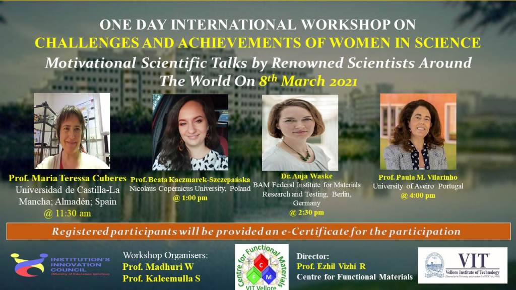
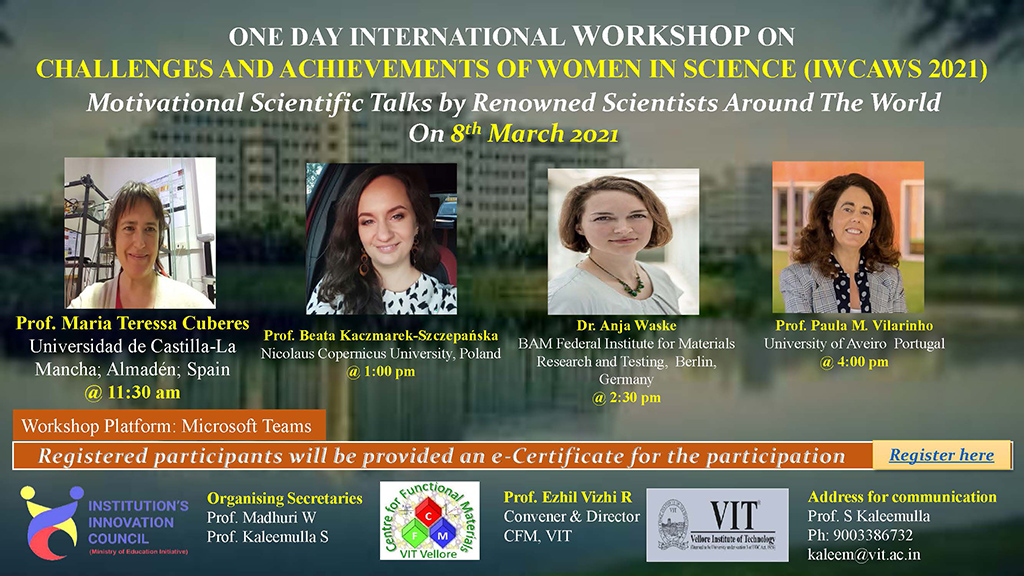
One Day International Workshop on Challenges and Achievements of Women in Science
Motivational Scientific Talks by Renowned Scientists Around The World On 8thMarch 2021
CFM-Workshop

Session 1 (@ 11:30 am)

Title: Learning About Materials on the Nanoscale with Scanning Probe Microscopes

Prof. Maria Teressa Cuberes
Universidad de Castilla-La Mancha; Almadén; Spain

Read Abstract

Scanning Probe Microscopy (SPM) provide invaluable tools for the characterization and manipulation of materials on the nanoscale. In this Seminar I will introduce the basics of these techniques and illustrate some SPM-based procedures which I have contributed myself to develop along my scientific career. In particular, I will discuss the technique of Ballistic Electron Emission Microscopy (BEEM), and its possibilities for the characterization of the electronic response at semiconductor interfaces [1], and other possible applications. In addition, I will share several examples of the use of Scanning Probe Microscopy for the manipulation of individual molecules, and how to learn about materials self-assembling from this kind of experiments. [2] Eventually, I will introduce a the techniques of Atomic Force Microscopy with ultrasound excitation, and their application to study of nanoscale dynamic elastic, viscoelastic and adhesive properties on both hard and soft samples, and to provide subsurface information[3].

About the Speaker

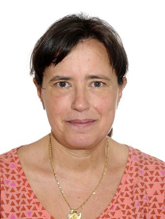
TeresaCuberesProf. Maria Teressa Cuberes
Degree in Physics (Materials Science) in 1987, and Ph.D. in Physics in 1991, in the University Complutense of Madrid, in Spain. Graduate student in the Materials Science Institute in Madrid (Consejo Superior de Investigaciones Científicas, CSIC) from 1987-1991. Postdoc in the Institute of Experimental Physics, in Berlin (Germany) from 1992-1993, in the Institute of Materials Science in Madrid (CSIC) from 1994-1995 and in IBM Zurich (Switzerland) from 1996-1997. Research assistant in the Department of Materials, University of Oxford (UK) from 1997-1998. Assistance Professor in the Engineering School of Almaden, University of Castilla-La Mancha (UCLM) from 1998-2000 Lecture in the Engineering School of Almaden (UCLM) from 2000-2003. Professor in Materials Science and Engineering in the Engineering School of Almaden (UCLM) from 2003 up to date. Research experience in Scanning Probe Microscopy techniques, semiconductor interfaces, thin polymer films and molecular layers, Ultra-High Vacuum, Synchrotron Radiation, Surface Spectroscopies, nanoscale electrical and mechanical properties.

  • 1. Cuberes, M.T.; Bauer, A.; Wen, H.J.; Prietsch, M.; Kaindl, G. Ballistic Electron Emission Microscopy Study of the Au/Si(111)7X7 and Au/CaF2/Si(111)7X7 interfaces. Applied Physics Letters 1994, 64, 2300-2302, doi:10.1063/1.111650.
  • 2. Cuberes, M.T.; Schlittler, R.R.; Gimzewski, J.K. Room-temperature repositioning of individual C60 molecules at Cu steps: Operation of a molecular counting device. Applied Physics Letters 1996, 69, 3016-3018, doi:10.1063/1.116824.
  • 3. Marino, S.; Joshi, G.M.; Lusuardi, A.; Cuberes, M.T. Ultrasonic force microscopy on poly(vinyl alcohol)/SrTiO3 nano-perovskites hybrid films. Ultramicroscopy 2014, 142, doi:10.1016/j.ultramic.2014.03.012.

Session 2 (@ 1:00 pm)

Title: Nanotechnology in cosmetics - opportunities or challenges?

Prof. Beata Kaczmarek-Szczepańska
Nicolaus Copernicus University, Poland

Read Abstract

Nanotechnology found application in cosmetics. They provide many advantages as high activity, transparency, solubility, etc. However, there are many concerns about the safety of such nanocosmetics. During the lecture, I will discuss the regulations of nanoparticles used in the cosmetic industry, as well as the opportunities and challenges of their application in cosmetics.

About the Speaker

TeresaCuberesDr. Beata K Szczepanska
Working as assistant professor in the department of Biomaterials and cosmetic chemistry at Nicolaus Copernicus University, Poland. Dr. Beata is a very active researcher and has completed 5 funded research projects and a project is in force funded by the Poland National Science Centre. Dr. Beata has published more than 55 research articles and 3 book chapters.

She is Editorial Board Member of Current Cosmetic Science journal (Bentham Science); Guest Editor in Special Issue "Biopolymers: Synthesis, Properties and Biological Applications" (Materials journal, Guest Editor in Special Issue "Thin Films for Biomedical Application"


Session 3 (@ 2:30 pm)

Title: X-ray Non-destructive testing of materials and composites

Dr. Anja Waske
BAM Federal Institute for Materials Research and Testing, Berlin, Germany

Read Abstract

Using magnetic materials for energy conversion as an example, this lecture shows how X-ray tomography investigations can contribute to structure elucidation in composites and solid samples. The components are tested non-destructively in order to characterize cracks, pores and other defects and their influence on the functional properties three-dimensionally and in good time in the life cycle of the material. If one combines microtomography with other methods of magnetic material characterization, unique statements about the structure and the functional properties are possible.

About the Speaker

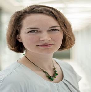
TeresaCuberesDr.-Ing. Anja Waske
Head of division "Radiological Methods" at the Federal Institute for Materials Research and Testing (Bundesanstalt für Materialforschung und -prüfung, BAM), Berlin. She studied physics at the Technische Universität Dresden, Germany, followed by a PhD degree in the field of X-ray tomographic characterization of granular matter. Her research field is at the interface of materials science and X-ray imaging. Her group develops 3D X-ray imaging methods and analysis routes for 3D image data for understanding the properties of functional, structural and additively manufactured materials.


Session 4 (@ 4:00 pm)

Title: Spark Plasma Texturing: a technology development for lead free pioezoelectrics

Prof.Paula M. Vilarinho
University of AveiroPortugal

Read Abstract

This talk addresses the sintering of undoped lead free piezoelectric (K1-xNax)NbO3 (KNN) ceramics by Spark Plasma Texturing (SPT) and compares their properties with equivalent ceramics prepared by Spark Plasma Sintering (SPS). I will describe the interplay between materials structure, microstructure, electrical conductivity, and non-linear dielectric properties for SPT KNN and the implications of these relations for enhancing electrical properties. Functional oxides, which include piezoelectric ceramics, are used in a wide variety of applications, from industrial machinery to compact electronic equipment and tools. Moreover, the Internet of Things is becoming a commodity, thus increasing the need for sensors and actuators. Consequently, it is expected that the overall market for piezoelectric devices will reach $31.33 billion by 2022. KNN is one of the most promising lead-free piezoelectric system to replace lead based piezoelectrics, mainly due to its high Curie temperature. Dense KNN ceramics require relatively high sintering temperatures, not compatible with the high vapour pressure of alkaline elements and thus alternative processing techniques are required. In this work we exploited the use of one derivative method of SPS that is Spark Plasma Texturing (SPT) defined as an edge-free SPS. We conclude that d33 (108 pC N-1), g33 (21.2×10⁻³ Vm N-1), Pr (19.7 μC cm-²) and Ec (11.9 kV cm-1) are significantly improved in undoped KNN ceramics processed, SPT. SPT KNN ceramics have a more homogeneous electrical microstructure with small grain size and narrow grain size distribution. SPT, as with hot-forging, results in neck destruction, particle rearrangement, and destruction of agglomerates improving the density and limiting grain coarsening, affecting point defects creation / distribution, giving rise to a rather homogeneous defect distribution. Consequently, SPT KNN ceramics grain cores and shells have similar resistance and capacitance behaviours. We hypothesise that, the electrical homogeneity of SPT KNN ceramics may along with the smaller grain size and higher density increase electric breakdown strength (EBDS) (of high relevance for industrial applications). In addition, the resultant compressively stressed lattice enhances the dielectric and piezoelectric performance.

About the Speaker

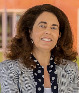
VilarihoProf.Paula M. Vilarinho
Vilarinho is Associate Professor at University of Aveiro (UA) since 2000 and a Senior Researcher of Associate Laboratory, CICECO – Aveiro Materials Institute. Currently she is: i) leader of the Electroceramics Group, within CICECO, ii) President of the Portuguese Society of Materials (SPM), iii) Coordinator (Portugal) of the Emerging Technologies Program within The University of Texas at Austin – Foundation for Science and Technology (FCT) Portugal Program, iv) Member of the Scientific Committee of the Doctoral Program in Materials Science and Engineering, UA. She was Visiting Professor at Dep of Materials Science and Engineering of North Carolina State University, USA, 2001, Visiting Professor at Dep of Materials Science and Engineering, University of Sheffield, United Kingdom, 2008 and Visiting Professor at McKetta Dep of Chemical Engineering, University of Texas at Austin, Texas, USA, 2015. She was: i) Director of Undergraduate Course in Ceramics and Glass Engineering, UA (1999-2001), and Director of Undergraduate Course in Materials Engineering, UA (2009-2016), ii) coordinator of Scientific Commission of Dep of Ceramics and Glass Engineering, UA (2002-2006), iii) former President of Portuguese Society of Microscopy (2010 - 2011), iv) former vice-president of Portuguese Materials Society (SPM) (2009-2013). She is: i) member of the Editorial Board of Scientific Reports (Nature Publishing Group), Processing and Application of Ceramics and International Scholarly Research Network - ISRN Ceramics, ii) member of Portuguese, European and American Materials Research Societies and Microscopy Societies, iii) referee in the selection of Portuguese and European R&D projects and National Science Foundation (NSF) USA, as well as a frequent referee of SCI journals. Vilarinho published over 295 papers, 6 book chapters, with ca. 5424 citations (h-index 38), 10 patent applications and edited 4 books. She has given over one hundred scientific and technical talks at international conferences and 135invited talks. She has(is) supervised(ing) 20 post-docs, 25 PhD students and 46 Master students. She has been involved and coordinating more than 20 R&D projects and in more than 20 European R&D actions, networks and projects on the development and characterization of dielectric, piezoelectric and ferroelectric materials. She organized 8 and co-organised 6 International Scientific Meetings and more than 12 National and International workshops on Materials Science topics. She was distinguished with the prize “Estímulo à Excelência” (Stimulus to Excellence) in February 2007 awarded by the Portuguese Foundation for Science and Technology (FCT). Her profile and scientific career were recently distinguish in the recent book “Successful Women Ceramic and Glass Scientists and Engineers: 100 Inspirational Profiles” by Lynnette Madsen, Willey, 2016. Vilarinho Research Group is engaged in fundamental and applied research in the synthesis, properties and processing of functional materials for electronics, microelectronics and related applications; mainly focused on electrical polarization phenomena in solids, aiming to understand mechanisms that control electrical polarization at the macroscopic and nanoscale level, and applying such understanding to the development of advanced nano and microelectronic devices. Her group has been using electrical and structural characterization tools (impedance spectroscopy, piezo- ferroelectric analysis, scanning probe microscopy, electron microscopy, Raman spectroscopy, etc) at the highest level. Materials under investigation include perovskite type ferroelectric, piezoelectric, dielectric and multiferroic oxides and piezoelectric polymers (PLLA, PVDF). Applications include microelectronic devices as memories, sensor and actuators, energy harvesters, thermoelectric devices, tunable dielectrics, but also and more recently biorelated uses, as bio-compatible piezoelectric platforms for tissue growth, biosensors, etc. The synthesis of nanofunctional materials in different geometries (1D, 2D, 3D) at low temperatures for compatible materials integration and using low cost approaches is becoming increasingly important in her´s research . Vilarinho´s group has been exploiting hydrothermal synthesis, diphasic sol precursors, photo chemical solution and electrophoretic deposition (EPD) for preparation of nanoparticulates, nanocomposites, thin, thick films of functional materials. More recently initiated exploitation of low-temperature budget processes, as FLASH sintering, and Cold Sintering. One of the newest R&D interests of Vilarinho group is related with Additive Manufacturing of ceramic and composite materials. The aim is on one side to explore techniques as 3D Printing and Robocasting for the fabrication of ceramic materials in direct collaboration with Portuguese Ceramic companies, on the other hand to explore Additive Manufacturing of functional ceramics and composite materials for microelectronics.


Interested are requested to register through the link given below.
The registered attendees will be provided an e-certificate for participation in the workshop.
Click Here for the Registration Link

Join here for the meeting with MS Team